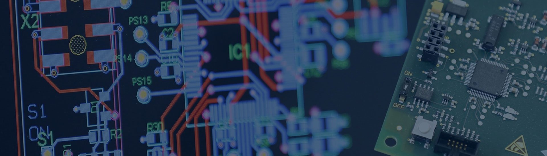
Pcb design pcb layout and circuit design Circuit Diagram Introduction Printed circuit board (PCB) layout design is a complex engineering art involving the layout of components and interconnections on a PCB to realize the circuit schematic functionality. A good PCB layout ensures proper signal and power integrity, electromagnetic compatibility, thermal management, manufacturability, and reliability of the product. This article provides a step-by-step Learn how to use EasyEDA to create a schematic and a PCB layout for an audio amplifier project. Get tips on PCB optimization, shape, size, layers, and grounding.
Learn the basics of PCB design with this guide that covers circuit diagram, schematics, board layout, PCB manufacturing, and soldering. Follow the steps and tips to make your own PCB with KiCad software and online services.
How to Design a PCB Layout Circuit Diagram
Printed circuit board (PCB) design can be easy with the right tools. See how the right layout software can save you time on your PCB board design, whether you are brand new or highly experienced. Printed circuit board (PCB) design and layout is both an art and a science, and it can be difficult to get started designing a new circuit board The pre-layout stage is a critical preparatory phase before starting the physical PCB layout design. During this stage, you focus on ensuring that the design is practical, manufacturable, and aligned with the project's technical and budgetary requirements. Proper preparation at this stage helps avoid costly design revisions and manufacturing
Lecture 06 -PCB Layout 2/2 | pcb.mit.edu yaypcbs@mit.edu. IAP 2025. Basic PCB Layout. Design Flow. Mechanical • Board shape • Mechanical Features • Stackup. Placement • Rooms/Blocks • Keep-out zones • Individual component arrangement. Routing • Trace routing • Copper pours. Verification • DRC Report • Simulation. Repeat as Learn how to design a PCB layout with this comprehensive guide that covers the essential aspects of PCB design, from schematic capture to design verification. Find out the best practices, tips, and guidelines for optimizing signal flow, power distribution, thermal management, and more.
Complete Guide to PCB Layout Design: Tips, Basics, & Guidelines Circuit Diagram
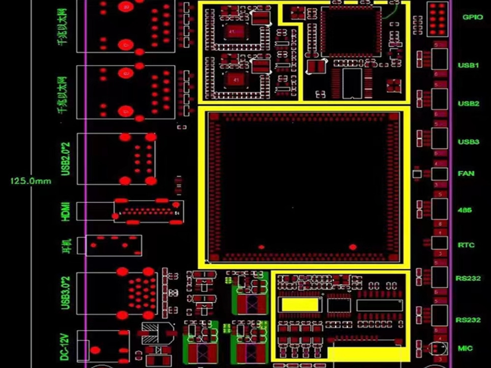
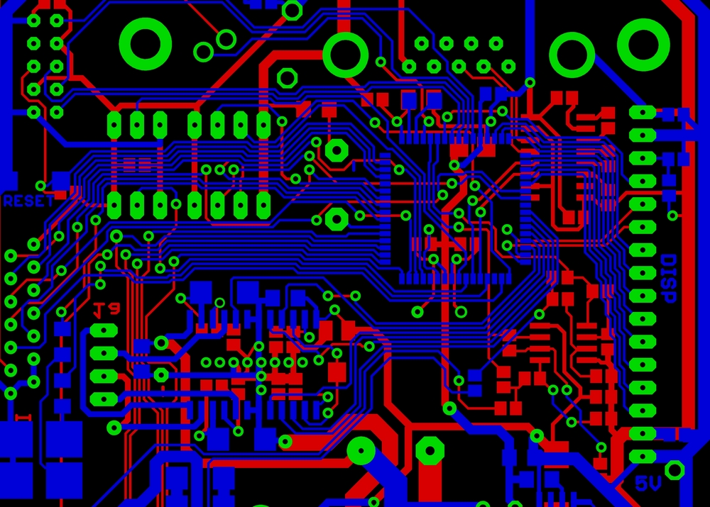
This section addresses common questions that newcomers to PCB layout design often have, providing clear and concise answers to facilitate a better understanding of the subject. What exactly is PCB layout design? PCB layout design is the process of arranging electronic components and their interconnections on a printed circuit board. Step 3: PCB layout stage. The PCB layout stage includes setting up the design tool, board outline, netlist import, component placement, routing, silkscreen cleanup, DRC check, and generating documents for production (Gerbers, netlist, etc.). Setting up the stack-up. The board layout is started by setting the stack-up and design rules. Learn how to create efficient and reliable PCB layouts with this comprehensive guide. Follow the steps and best practices for schematic entry, component placement, routing, stackup, DFM, and more.
